
 Technology In PCBA Processing")
The role of Automatic Optical Inspection (AOI) inspection
AOI is a kind of inspection equipment, also known as AOI optical automatic inspection equipment, has become an important inspection tool and process quality control tool to ensure product quality in the electronics manufacturing industry.AOI inspection equipment works in the automatic inspection process, the AOI inspection equipment machine automatically scans the PCBA product through the high-definition CCD camera, collects images, compares the test points with the qualified parameters in the database. After image processing, check out the defects of the solder joints on the target PCBA, and by displaying or automatically marking the defects. For maintenance personnel to repair and SMT process personnel to improve process parameters.
AOI system includes a variety of light source lighting, high-speed digital camera, high-speed linear motor, precision mechanical drive structure and image processing software. Testing, AOI equipment through the camera automatically scan and PCB, PCB components or special parts (including the state of the printed solder paste, SMD components, solder joint shape and defects, etc.) to capture images, through the processing and database software to compare the qualified parameters, and a comprehensive judgment of components and characteristics are qualified, and then test conclusions, such as missing components, bridging or solder joint quality problems.
AOI works in the same way as the vision systems used in SPI and printing presses among SMT, usually using design rule checking (DRC) and pattern recognition. the DRC method checks circuit patterns against some given rules (all lines should end at the solder joint, all leads should be at least 0.127 mm wide, all leads should be at least 0.102 mm apart, etc.). This method can algorithmically ensure the correctness of the circuit to be tested and is used by many because of its simplicity of production, simple algorithm logic, fast processing speed, small amount of program editing, and small space occupied by data. However, the ability of the method to determine the boundary is poor.
The graphical recognition method compares the stored digital image with the actual image. The inspection is performed based on the complete printed circuit board or the inspection file created from the model, or based on the inspection program prepared in computer axis-aided design. Its accuracy depends on the adopted licensing rate and inspection procedure, which is generally the same as the electronic test system, but the amount of data collected is large and the real-time processing of the data is required. The pattern recognition method has obvious advantages by using actual design data instead of the design principles already established in the DRC.
AOl has the functions of component inspection, PCB board inspection, soldered component inspection, etc. The general procedure of AOI inspection system for component inspection is to automatically count the printed circuit board with installed components and start inspection; check the lead side of the printed circuit board to ensure that the lead ends are aligned and bent correctly; check for missing parts, wrong parts, damaged parts, check the type of installed IC and discrete devices, the orientation and location, and check the quality of marking printing on IC devices. If AOI finds a defective part, the system sends a signal to the operator or triggers a process that automatically removes the defective part. The system analyzes the defects, provides the host with the type and frequency of defects, and makes the necessary adjustments to the manufacturing process. the efficiency and reliability of AOI inspection depends on the integrity of the software used. the AO also has the advantage of being easy to use, easy to adjust, and does not require the writing of visualization system algorithms.
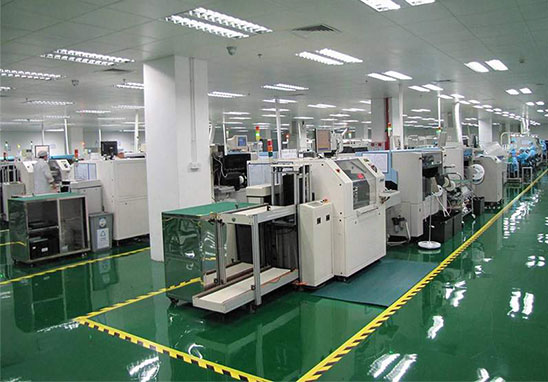
Our PCBA processing advantages
Grande has its own SMT chip processing factory, which can provide SMT chip processing service for the smallest package 0201 components. The SMT factory is equipped with 3 Fuji high-speed placement lines, 2 DIP plug-in production lines, with AOI optical detector, automatic solder paste printer, semi-automatic solder paste printer, lead-free wave soldering, leaded wave soldering, upper and lower 8-temperature reflow soldering, PCBA functional test rack, aging, board carrier, cleaning tools, etc. Meanwhile, we have set up a professional R&D laboratory with 5 professional engineers to cooperate with customers for general At the same time, we have set up a professional R&D lab with 5 professional engineers to cooperate with customers to conduct general function tests, test point tests, as well as path, noise, waveform, drop and temperature tests.