

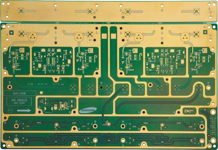
6 Layers Hi-frequency Blind Via board
We're a leading PCB and PCBA manufacturer in China, offering a full range of PCBs and PCBA boards for most applications. All products are manufactured under strict quality control system. OEM, ODM, and EMS service is available for PCBA production.
We're a leading PCB and PCBA manufacturer in China, offering a full range of PCBs and PCBA boards for most applications. All products are manufactured under strict quality control system. OEM, ODM, and EMS service is available for PCBA production.
HesconPCB is a printed circuit board manufacturer based in China. The company offers custom prototype to audio application production PCB fabrication.
1. Automated equipments to reduce the cost ;
2. Our prices are very competitive and quality is super ;
3. Fast action/24hours quotation ;
4. Quick prototyping and production .
Make an notion resolution for optimizing your electronic devices. WonderfulPCB rigid PCB boards are readily available in 1-28 layers, created of CEM-1, CEM-3, FR-4, FR4 Halogen free, Higher TG, Rogers material and in line with the board thickness of 0.21mm to 7.0mm, our PCBs is often separated into different category which include computers, televisions, mobile phones and so on.
Specfication
Base Material: FR-4, CEM-1, CEM-3, High TG, FR4 Halogen Free, Rogers
Number of Layers: 1-28 Layers
Board Thickness: 1.6 mm
Copper Thickness: 0.5 OZ to 7.0 OZ
Min. Hole Size: 3mil (0.075mm)
Min. Line Spacing: 3mil (0.075mm)
Min. Line Width: 3mil (0.075mm)
Surface Finishing: HASL / HASL lead free, HAL, Chemical tin, Chemical Gold, Immersion Silver/Gold, OSP, Gold plating
Solder Mask Color: Green/Yellow/Black/White/Red/Blue
Certificate: UL, ISO 9001, ISO 14001
Application
Rigid PCBs are used widely for Communications, Computers, Medical equipments and Consumer electronics.
Our Production Capability for PCB
Layer: 1 to 28 layers
Material type: FR-4, CEM-1, CEM-3, High TG, FR4 Halogen Free, Rogers
Board thickness: 0.21mm to 7.0mm
Copper thickness: 0.5 OZ to 7.0 OZ
Copper thickness in hole: >25.0 um (>1mil)
Size:
- Max. Board Size: 23 × 25 (580mm×900mm)
- Min. Drilled Hole Size: 3mil (0.075mm)
- Min. Line Width: 3mil (0.075mm)
- Min. Line Spacing: 3mil (0.075mm)Surface finishing: HASL / HASL lead free, HAL, Chemical tin, Chemical Gold, Immersion Silver/Gold, OSP, Gold plating
Solder Mask Color: Green/Yellow/Black/White/Red/Blue
Tolerance
- Shape tolerance: ±0.13
- Hole tolerance: PTH: ±0.076 NPTH: ±0.05PCB Packing
- Inner packing: Vacuum packing / Plastic bag
- Outer packing: Standard carton packingCertificate: UL, ISO 9001, ISO 14001
Special requirements: Buried and blind vias+controlled impedance +BGA
Profiling: Punching, Routing, V-CUT, Beveling
Provides OEM services to all sorts of printed circuit board assembly as well as electronic encased products.

| Name: | |
| layers: | 6 |
| thickness: | 2.0mm |
| Min line width/space: | 0.15/0.15MM |
| Min hole size: | 0.5mm |
| Copper Thickness: | 3oz |
| Surface finish: | ENIG |
| Material: | RO4350B |
| Blind hole: | L1-3, L1-4 |